TITLE:
LAB REPORT HALF ADDER PRACTICAL
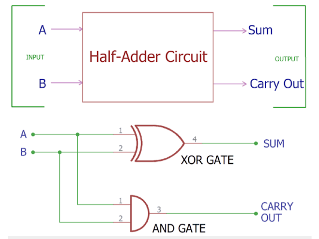
INTRODUCTION: A half adder is a
type of adder, an electronic circuit that performs the addition of numbers. The
half adder is able to add two single binary digits and provide the output plus
a carry value. It has two inputs, called A and B, and two outputs S (sum) and C
(carry). The common representation uses a XOR logic gate and an AND logic gate.
TRUTH TABLE:
|
X |
Y |
S |
C |
|
0 |
0 |
0 |
0 |
|
0 |
1 |
1 |
0 |
|
1 |
0 |
1 |
0 |
|
1 |
1 |
0 |
1 |
CIRCUIT
DIAGRAM:
HYPOTHESIS:
How can we perform the addition of two bits. In this
practical we make the logical circuit diagram of half adder. Main purpose of
making this half adder addition check the diagram step by step and perform the
logical expressions.
EQUIPMENT'S:
ü Electronic workbench
ü ex or gate
ü and gate
ü switches (2)
ü led (2
ü ground
ü vcc
PROCEDURE:
The Half Adder logic circuit diagram can be made by
combining the exclusive OR gate and (AND gate)
providing same inputs to the both gates. We get the sum output across EX-OR gate and
carry out bit across AND gate.
The Boolean
expression of half adder circuit:
Sum= x’y+xy’
Carry= xy
RESULTS &
DISCUSSION:


No comments:
Post a Comment